Kicad - Design
Note this is an older doc I’ve kept for info, it’s better to use the Gerber files with FlatCam instead because it’s easier and has more features
PCB Design
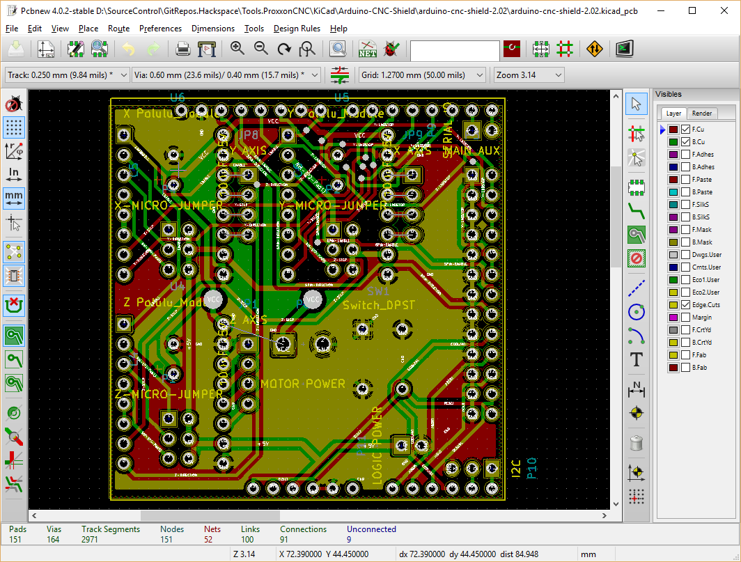
The first step is to open the PCB Design within KiCad
Export Top Layer
Next we’re going to export the top layer as an SVG image
| Notes |
|---|
| It’s best to avoid the use of the File -> Export Svg option since that doesn’t allow for a negative to be created, instead we’re going to use Plot |
| It’s also best to draw a square around the board on the “Edge Cuts” Layer, make sure it doesn’t come into contact with any of the pins |
- Select File -> Plot
- Select the Front Copper Layer on the left
- Select the Output directory “svg/”
- Select Drill marks: Small
- Negative plot: Ticked
- Mirrored Plot: Unticked for the front layer
- Exclude PCB edge layer from other layers: Unticked To include the Outer cut line
Click Plot to export the svg
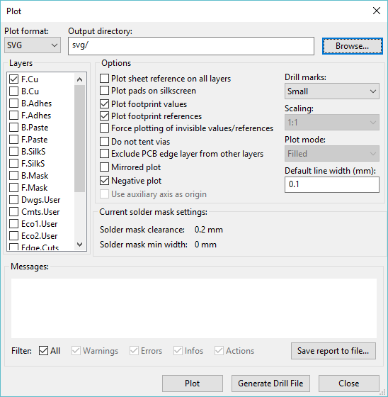
Export Bottom Layer
Next for the bottom layer repeat as above but make the following changes
- Select the Bottom Copper Layer on the left, unselect the Front Layer
- Mirrored Plot: Ticked for the bottom layer
Click Plot to export the svg
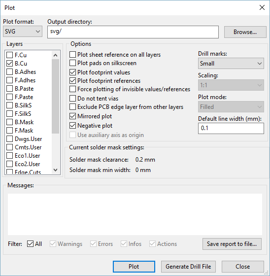
Inkscape Edit
Next we need to resize a couple of things within inkscape.
First we want to resize the actual Document
- Open each svg within inkscape
- Open up File -> Document Properties
- Select the white box surrounding the Board
- Expand the Resize page to content…
- Click Resize page to drawing or selection with the white outer box selected
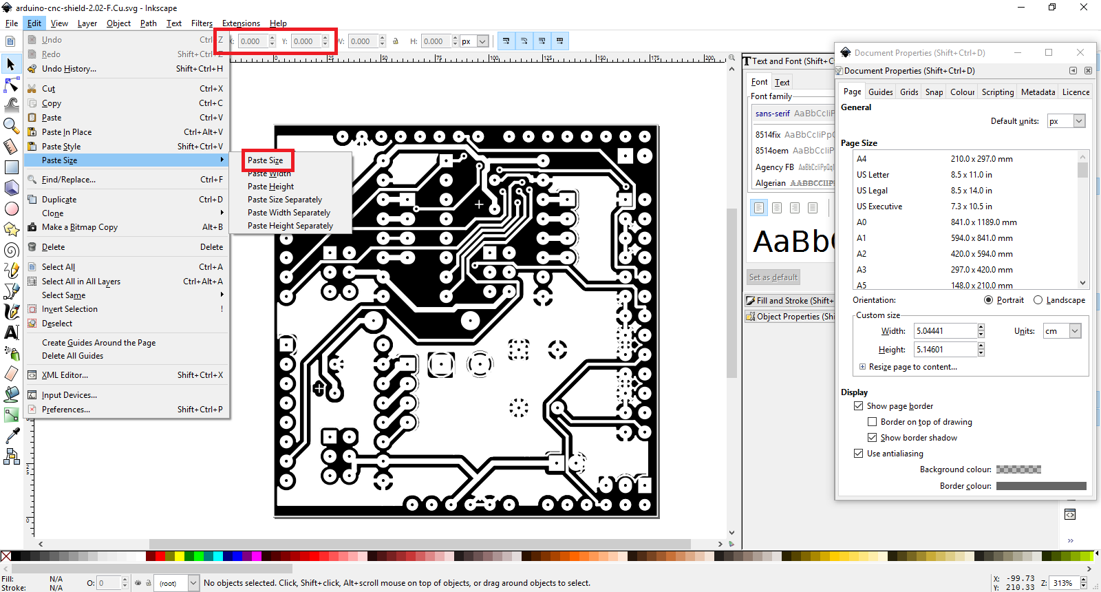
Next we need to resize the big black box that surrounds the box so that it fits within the document, this is acting as a mask
- Select the white outline box, and select Edit -> Copy
- Select the Outer black box and Select Edit -> Paste Size -> Paste Size
- At the top Enter X: 0 Y: 0 to position the box at the bottom left corner
Examples
Some svg’s of adafruit’s pcb ruler for testing how small can we go
A test of the pcb I replicated from the arduino cnc project, I’ve got no plan on using this (just created it to confirm the wiring is what I thought it was), but maybe a good test
TODO
- None of this is tested so far
- One suggestion is that lines should be no thinner than 1.5pt, 5pt font. Further experimentation is needed
- I could do with trying to print adafruit’s PCB ruler as a test.