KiCad Design Rules - TODO
Next we’re going to set the design rules for the board.
Hackaday Suggestions
Looking at this hackaday link for boards made using a Laser Cutter. Its suggests the following
| Rule | Min | Typical | Max |
|---|---|---|---|
| Track Clearance | 15mil (0.381mm) | ||
| Track Width | 22mil (0.5588mm) | ||
| Drill size | 20mil (0.508mm) | ||
| Vias / Outer | 18mil (0.4572mm) | 20mil (0.508mm) | |
| Pads Top / Bottom | 15mil (0.381mm) | ||
| Autorouting Grid | 2mil (0.0508mm) |
They also suggest
- 24 gauge wire or thinner is used for Vias
- Drill bit is 0.02” (0.508mm) in diameter for via holes
- Drill bit is 0.04” (1.016mm) in diameter for header pin holes
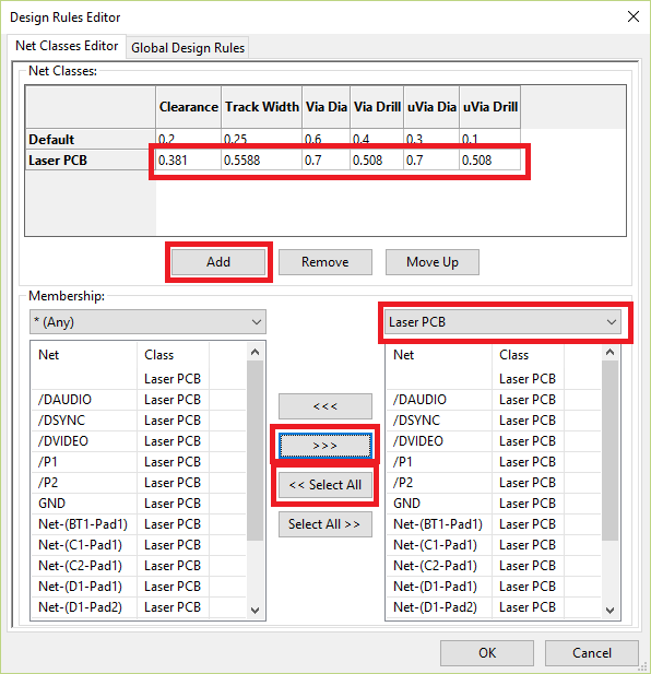
Kicad Design Rules
By Selecting Desgin Rules -> Design Rules from the menu we can create a new NetClass to add in values You may want to play around with different smaller values to see what is possible.
| Header | Value |
|---|---|
| Name | Laser PCB |
| Clearance | 0.381 |
| Track Width | 0.5588 |
| Via Dia | 0.7 |
| Via Drill | 0.508 |
| uVia Dia | 0.7 |
| uVia Drill | 0.508 |
Also you need to apply this netclass to all the components on the list